Pocket Frequency Meter
A four-digit frequency counter built on an 8051-compatible microcontroller (STC89C52RC). The project covers the whole stack of a small embedded instrument: 120 lines of C51 firmware, a schematic drawn in six functional blocks, and a two-layer board. It was built in 2025 as coursework and is kept as a finished record under MIT, in the repository.
The measurement principle, the accuracy it can reach and the limits of the method are all visible in the firmware at once. The part I went furthest into is the timer constant that sets the gate, and why matching it to the crystal on the board was the better fix.
How it measures
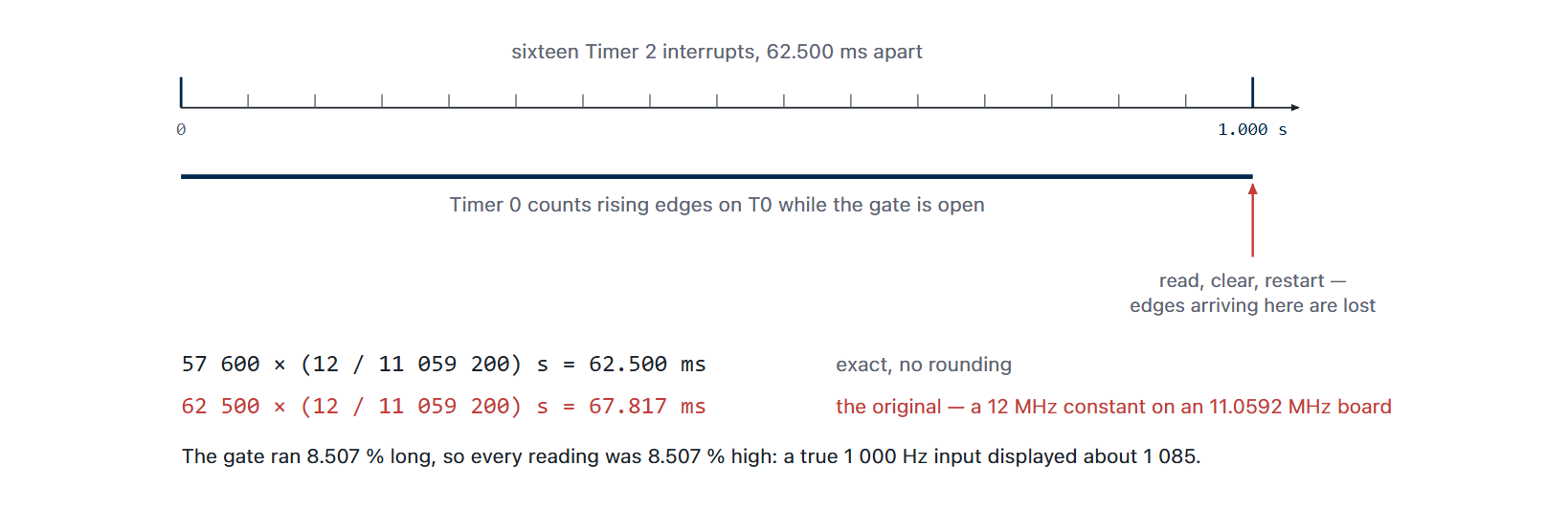
The instrument implements the classic direct-count method: count the rising edges of the input for a gate of exactly one second, and the count is the frequency in hertz. Two hardware timers divide the work.
- Timer 0 runs as an external event counter in 16-bit mode on the T0 pin (P3.4), with an interrupt on each overflow so counts beyond 65,535 keep accumulating. The pair (overflow count,
TH0:TL0) spans 32 bits. - Timer 2 runs in auto-reload mode and interrupts every 62.5 ms. Sixteen interrupts close the one-second gate, at which point the counter is stopped, read, converted and restarted.
void timer2(void) interrupt 5 {
    TF2 = 0;                       // Timer 2 does not clear its own flag
    if (++time == 16) {            // 16 × 62.5 ms = 1 s
        time = 0;
        TR0 = 0;                   // close the gate
        fre = (unsigned long)count * 65536 + ((TH0 << 8) | TL0);
        count = 0;  TH0 = 0;  TL0 = 0;
        TR0 = 1;                   // reopen
    }
}
The main loop does nothing but refresh the multiplexed display—four digits at about 1 ms each, blanking the segment bus between digits so the pattern for one digit is never briefly visible on the next. The gate comes from Timer 2 and is unaffected by anything the main loop does.
Four parts, one owner each
The instrument is small enough that its whole structure fits in one sentence, and I built it so that it would: a timebase, a counter, a readout and a supply, each owned by exactly one piece of hardware and one piece of code.
- Timebase. Timer 2 in auto-reload, one constant, one interrupt. It owns the definition of a second and nothing else touches it.
- Counter. Timer 0 in external-event mode on T0, plus an overflow counter in software. The pair spans 32 bits, so the count is never the thing that runs out.
- Readout. A four-digit multiplexed display refreshed by the main loop, roughly a millisecond a digit, with the segment bus blanked between digits.
- Supply and entry. USB-C behind a slide switch, a reset network, and the port headers that make every pin reachable with a probe.
The division is what makes the accuracy argument possible. Because the gate lives entirely in an interrupt and the display lives entirely in the main loop, no amount of work in the readout can lengthen or shorten a measurement; because the counter is hardware, no interrupt latency can lose an edge. Every error term on this page is therefore a property of the method or of a component, and none of them is a property of the code—which is the state a small instrument should be in before anyone quotes a number from it.
Setting the timebase
Matching the timer reload to the 11.0592 MHz crystal
The firmware derived its 62.5 ms tick from a Timer 2 reload of 62,500 machine cycles—correct only on a 12 MHz part. The schematic fits an 11.0592 MHz crystal, the usual choice for 8051 boards that need exact baud rates and almost certainly inherited from a general-purpose board layout. At that clock a machine cycle is 1.085 µs, so the tick was 67.8 ms, the gate was 1.085 s, and a true 1,000 Hz input displayed about 1,085. The error was systematic, roughly a hundred times larger than everything else on this page put together, and invisible to the firmware—an 8.5% error looks entirely plausible on a four-digit display.
The fix was one line, and it left the design better than the 12 MHz version would have been. Keep the crystal and change the reload to 57,600 cycles: 57,600 × 12 / 11,059,200 s = 62.500 ms with no rounding at all, whereas 12 MHz only ever gave 62.5 ms because 62,500 happens to be a round number. Swapping the crystal would also have worked, but it costs a part and gives up the board's exact-baud-rate property.
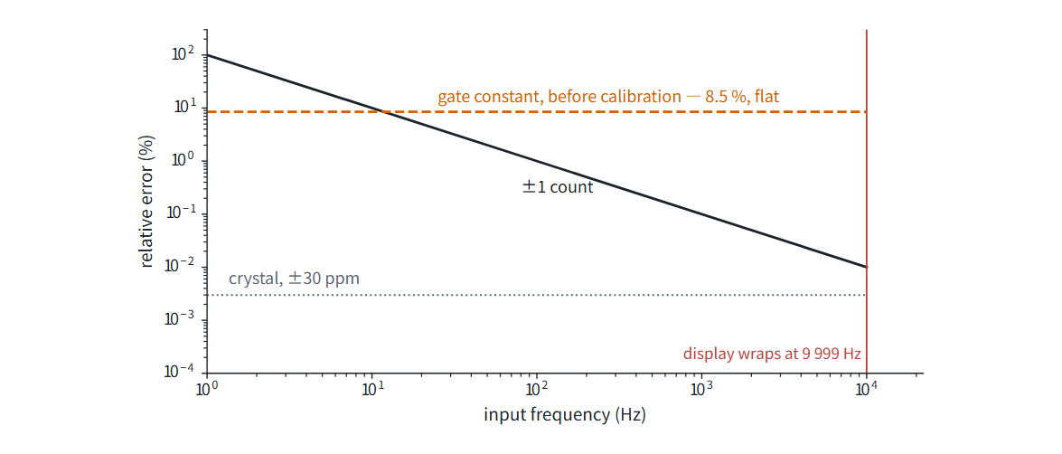
With the timebase fixed, the terms that remain are properties of the method and of the readout:
| Term | Size | Where it comes from |
|---|---|---|
| ±1 count quantization | ±1 Hz | The gate and the input are asynchronous, so the count can land either side of the true value. It is 0.02% at 5 kHz and 10% at 10 Hz, which is what sets the lower end of a direct counter's useful range. |
| Gate-blind window | A few µs per gate | Edges arriving between TR0 = 0 and TR0 = 1 fall outside the gate. The term is systematic and grows linearly with frequency. |
| Crystal tolerance | ±30 ppm | The timebase itself. It sits below the ±1-count floor for anything under about 33 kHz, and would become the dominant term in a reciprocal-counting version. |
| Display span | Four digits | The counter itself spans 32 bits. The readout is four digits, so 9,999 Hz is where the display, not the measurement, sets the ceiling. |
| Input threshold | Logic level | T0 is a digital pin with a fixed threshold, so the instrument is specified for a logic-level square wave and anything else is shaped ahead of it. |
So the readings are trustworthy from roughly 100 Hz to 9,999 Hz with a clean logic-level square wave: ±1 count is 1% at the bottom of that window and 0.01% at the top. Below it the ±1-count term dominates; above it the four-digit display range ends.
How the design was arrived at
The order of the work was chosen so that each decision was made against something already fixed rather than against an intention. The measurement method came first, because it decides everything downstream: direct counting fixes a one-second gate, the gate fixes what the timers must do, and the timers fix which pins are spoken for. Only then was the schematic drawn, and it was drawn as six separate blocks—supply, reset, crystal, key input, header breakout, MCU—so that each one could be checked as a unit instead of as part of one large net.
Simulation came next, against the schematic rather than the board, so that a wrong connection was found while it still cost a wire. The layout came after that, and the placement follows the blocks: the supply corner stays together at the left edge, the crystal sits hard against the XTAL pins because that is the one net on the board where trace length decides whether the circuit runs at all, and the DIP-40 sits in the middle with the headers along its long edges so every pin is reachable without lifting the board.
The board was then laid out twice from the same schematic: once as a general-purpose minimum system and once as the instrument. Keeping them as two layouts of one drawing rather than two drawings is what makes a change to the circuit a single edit. The enclosure was modelled last, after the outline was final, so its opening, wall thickness and internal clearance are taken from the layout rather than measured off a built board.
Hardware
The board is a compact STC89C52RC design: the MCU in DIP-40, an 11.0592 MHz crystal with its two 47 pF load capacitors, a 10 kΩ resistor network pulling up P0 (which is open-drain and cannot source current without it), a USB-C input behind a slide switch, a reset network, tactile switches on P3.2 and P3.3, and every port broken out to headers.
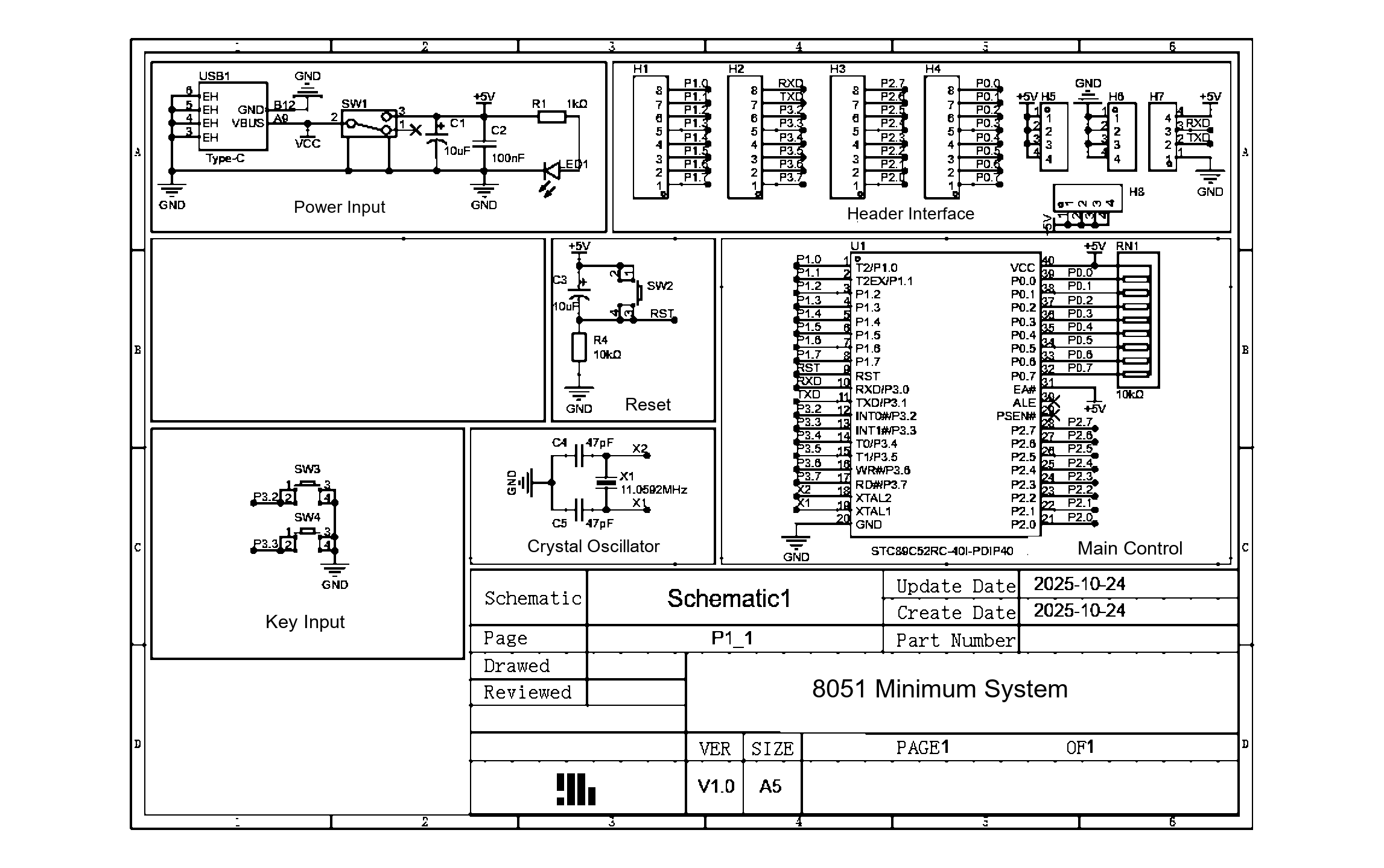
The sheet is divided rather than drawn as one net: power input, reset, crystal, key input, the header breakout, and the MCU. Each block stands alone—the reset network, the two load capacitors either side of the crystal, the resistor network on P0—so a question about the assembled board goes to one block rather than to the whole drawing.
The board is two-layer. Almost everything that has to reach a header runs on the top; the supply and the returns drop to the bottom, which is what keeps the header rows straight instead of bent around each other.
The layout puts the DIP-40 in the middle with the port headers along its long edges, so every pin is reachable with a probe without lifting the board. Power enters at the left—USB-C, slide switch, reset button together—and the crystal sits against the XTAL pins on the right, which is the one place on this board where trace length decides whether the circuit runs at all.
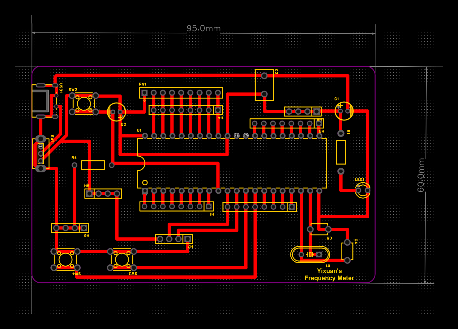
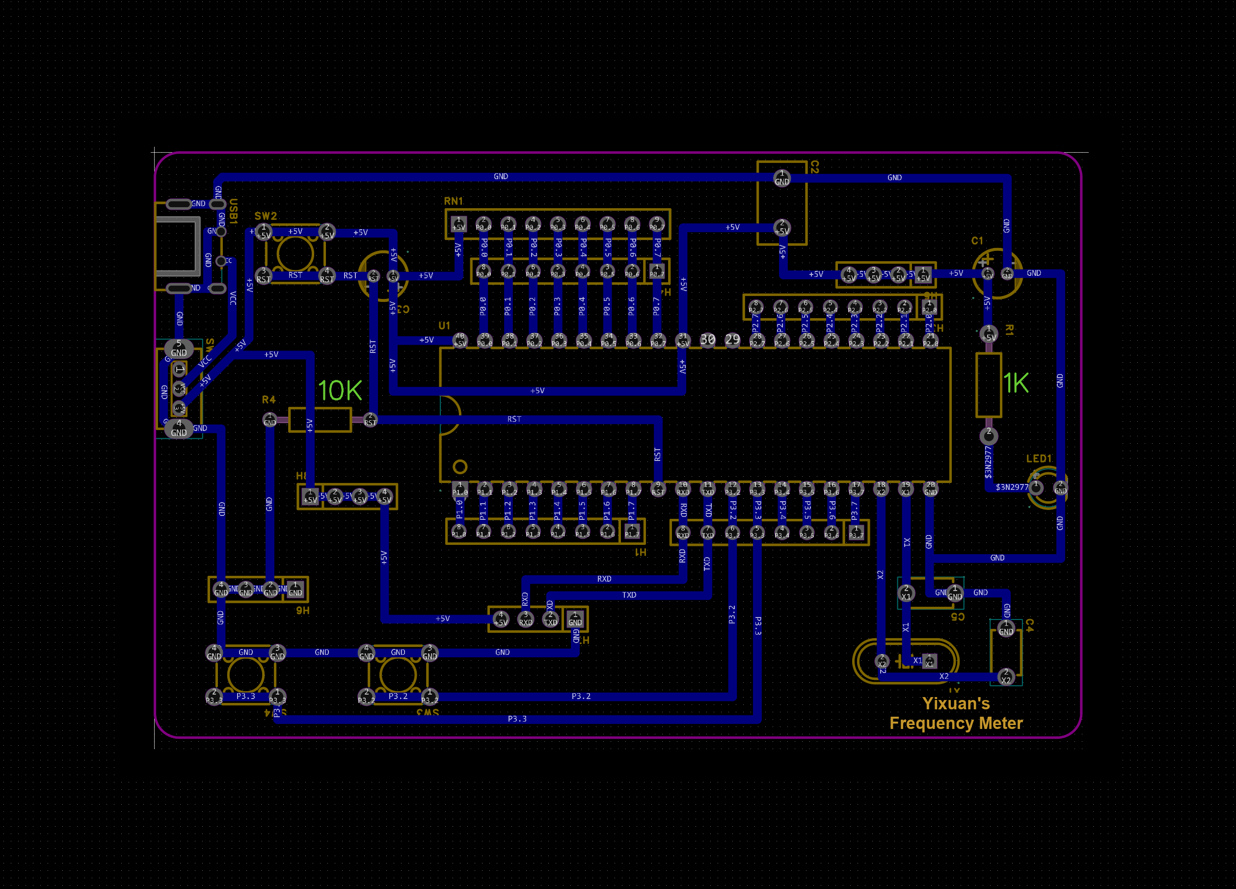
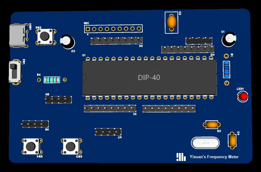
The same circuit went to the board twice. The first revision is a general-purpose STC89C52 minimum system at 90.0 × 50.2 mm, with mounting holes at the four corners and spare indicators, meant to carry any 8051 project. The instrument revision is the one above. Keeping them as two layouts of one schematic means a change to the circuit is made once.
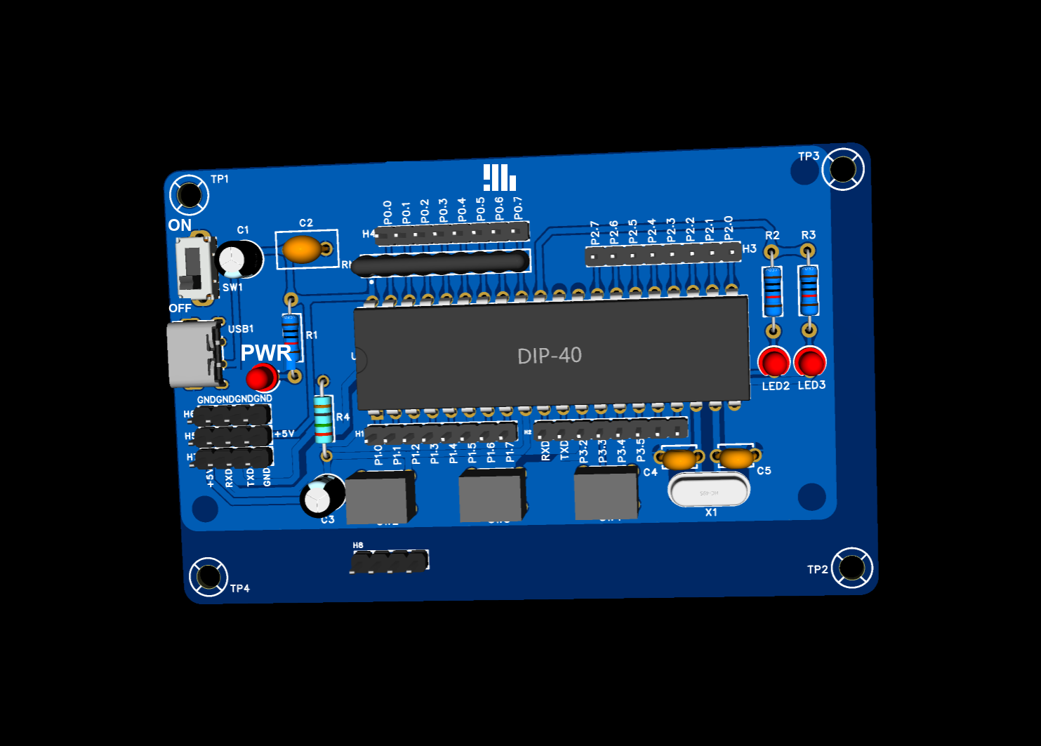
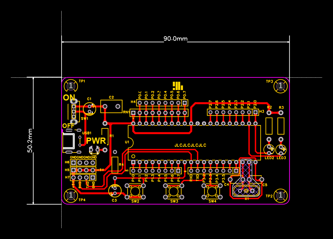
The instrument revision grew by 5 mm in each direction, which is what the fourth switch and the wider header field cost. Everything else—the supply corner, the reset, the crystal against the XTAL pins—carried across unchanged, because it is the same schematic underneath.
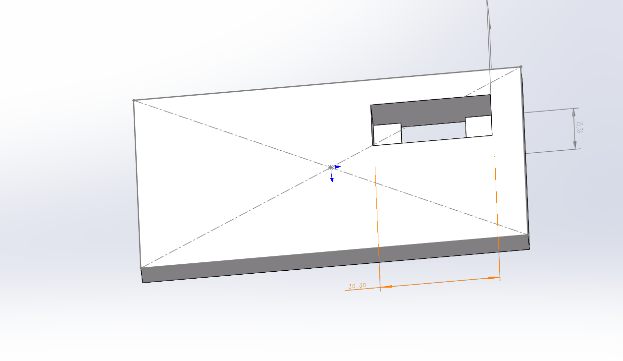
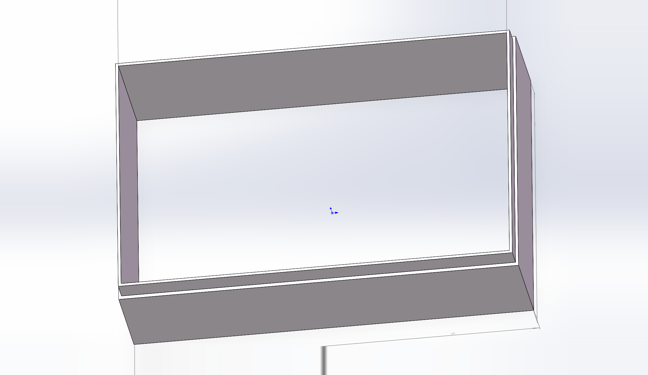
The last step was the box. Modelling it after the board outline was fixed meant the opening, the wall thickness and the clearance over the tallest part could all be taken from the layout rather than measured off a built board, which is the point at which a project stops being a bare PCB.
The measured signal arrives on P3.4 through the header breakout, which is where the counter input lives, and the firmware is what turns the board into an instrument.